SAHA INSTITUTE OF NUCLEAR PHYSICS
Department of Atomic Energy, Govt. of India
Metalorganic Vapour Phase Epitaxy (MOVPE)

Description:
Metalorganic Vapour Phase Epitaxy (MOVPE) or Metalorganic Chemical Vapour Deposition (MOCVD) is an epitaxial crystal growth technique used for growing high quality single crystalline thin films of different materials on different substrates. The MOVPE system at SINP is used for research in III-V compound semiconductor heterostructure materials for optoelectronic, photovoltaic and high speed electronic applications. These materials are comprised of different quantum structures, such as the quantum wells, wires and dots, all of which can be grown using this system. There are lot of scopes for research in improving and understanding the growth process of such materials. Among the various III-V semiconductors, AlGaAs/GaAs, GaInP/GaAs, InGaAs/InP, AlGaInP/GaAs etc material systems play important role in quantum well based optoelectronic device applications as well as study of fundamental quantum phenomena which are undertaken in the MOVPE laboratory of SINP.
Research Targets:
1. Role of interface roughness, barrier heights on optical properties of quantum well structures.
2. Electrical transport under quantum regime and two-dimensional electron gas
3. Growth of InAs/GaAs quantum dots and low temperature optical spectroscopy
4. Growth of free-standing InP nanowires
5. Device structures - Multi-junction solar cells, Heterostructure Bipolar Transistor
Some recent results from the MOVPE laboratory, SINP:
1. GaAs/AlAs Distributed Bragg Reflector (DBR):
DBRs are alternate multiple layers of high/low refractive indices, each designed for total reflection or absorption of a particular or a band of wavelength of light, which are used in designing various quantum devices such as lasers, high efficiency solar cells, detectors etc. Here is an example of growth of AlAs (35 nm) /GaAs (25 nm) DBR of 15 layers, designed for reflecting green light of the spectrum which is grown in our MOVPE system. Fig. 1 shows the three GaAs wafers in the MOVPE reactor - before and after the growth of the DBR structure. Fig. 2, 3 and 4 show the cross-sectional SEM image, x-ray rocking curve (done at the Photon Factory synchrotron radiation facility, Japan) and SIMS depth profile of the DBR structure, respectively.

Fg.1. GaAs wafers inside the MOVPE reactor before and after the growth of DBR structure.

Fig. 2 Cross-sectional Scanning Electron Microscopic (SEM) image of the DBR structure
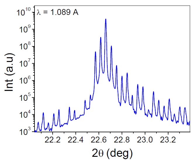
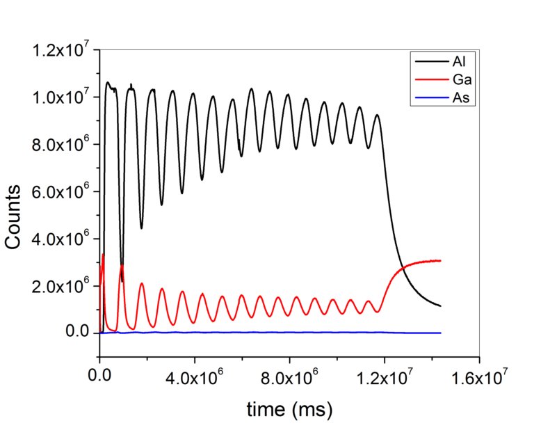
Fig. 3 and 4 – x-ray rocking curve and SIMS depth profile of GaAs/AlAs DBR structure
2. GaAs/AlGaAs multi-quantum wells (MQW)
Quantum well structures are realized in epitaxial systems by growing a thin a layer of low bandgap semiconductor (well) between two high bandgap (barrier) layers. Important parameters here are the uniform thickness, high crystalline quality, fluctuation at the interface, defect and impurity concentration. Here, we have grown three GaAs quantum wells of nominal thicknesses of 35 Ȧ, 55 Ȧ and 75 Ȧ with Al0.3Ga0.7As barriers of thickness 400 Ȧ in the same structure. Photoluminescence at different low temperatures showed distinct peaks corresponding to the three quantum wells as shown in Fig.5.
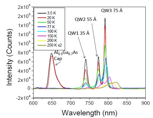
Fig. 5 Photoluminescence spectra of GaAs/AlGaAs multiple quantum well structure grown by the MOVPE system