SAHA INSTITUTE OF NUCLEAR PHYSICS
Department of Atomic Energy, Govt. of India
Design : |
|
The Frames |
|
 |
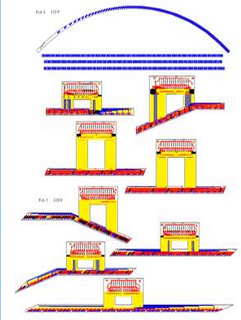
The frames have been made out of PEEKGF30 due to the low radiation length with high tensile strain and good machining properties. Each frame have been made of six pieces in order to reduce the material as well as the machining cost.These pieces were joined by lap joints to make one continuous frame . All the joints are made on the straight sections of the frame. The joining was done on a Master tooling plate using high precision reference pins, two in each segment, in order to obtain the desired dimension sand flatness of the assembled frames. This technology also ensures the dimensional reproducibility of all the assembled frames. |
Cathode PCB |
|
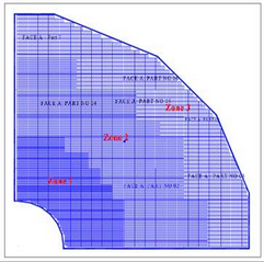 |
The Cathode planes are made by 0.4mm double sided Printed Circuit Board (PCB). Pad side is gold coated copper surface and solder side is connected to double-sided flexible Kapton PCBs. The cathode plan covers fully the 2-9 degrees span in the azimuthal angle. The cathode plane has Inner radius of 22.5 cm and outer radius of 119.5 cm. The Cathode PCBs (bending and non-bending) are segmented in three different size zones. |
The Kapton PCB |
|
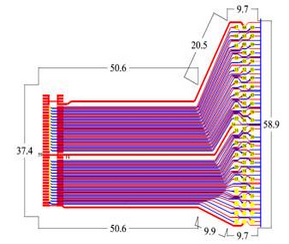 |
The connection between the readout pad of the cathode plane and the front-end readout card (MANU) are done by double-sided flexible Kapton PCB. Each PCB contains 67 connections on the cathode side of which three are grounded. The pads on the PCB of front-end readout card side, are connected to a 80 – pin connector. |
Anode PCB |
|
 |
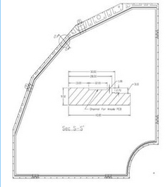
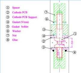
The Anode PCBs are embedded in the non bending(FACEA) side of the frames. It is a three layered board where the HV lines are through the middle layer, the pads are on the to player while the bottom layer consists essentially of a ground layer. The total thickness is 0.8mm. The to player is shown by red while blue lines are in middle layer, these are to connect the anode wires to the HV supply. Anode wires, in bunches of four are connected through a resistor (typically 2MΩ) and filtered with a 1nF capacitor. Each wire is stretched across by soldering (and gluing) it on the pads (2.5mm a part on horizontal direction) of a node PCB. There are twelve PCBs in each quadrant. The mechanical exit board The mechanical exit board is the outer skin for the sandwich and contains holes matching with holes on the rohacell. The exit boards are also machine dconventionally and the holes cut with dimensional accuracy of+/-0.5mm. Since the dimensions are identical or very similar to that of rohacell, similar tables of parameters measured are produced. |
The central point fixation |
|
 |
Two cathode planes in a quadrant have been bound together at a round middle of the quadrant(r=758mm) by the central point fixation, to reduce the deformation due to the gas over presser inside the quadrant. The central point fixation is made of PEEK-GF30, the fixation point is outside the high density hit zone since the point generates a dead zone. |
Electronic Bus board: |
|
 |
|
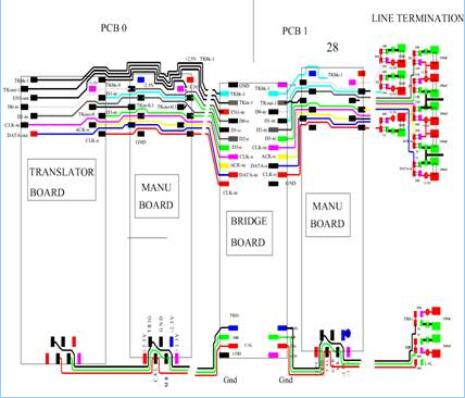
| This PCB couples the flexible PCB s from the cathode pads to the Front End Electronics. Each electronics board consists of 12 read out bus patch on which the MANU cards are mounted. Each bus patch is equipped with a translator board which sends control signal to Manas chips and line drivers on Bridge boards.Tha read out cards are mounted on the exit board using Samtech connector. For convenient of the fabrication this exit board was fabricated in nine pieces.The low voltage bus line of +2.5 volt and -2.5 volt and + 3.3 volt are placed on this pcb.for board MANAS and Mark chips respectively. | |
 |
|